Research Area
6.1 Imaging technologies
■Three-dimensional integrated imaging devices
We are researching imaging devices with a 3D structure in our quest to develop a next-generation image sensor having more pixels and a higher frame rate. These devices are fabricated by bonding a photodetector and a signal processing circuit which are formed on different substrates. They have a signal processing circuit for each pixel directly beneath the photodetector (Figure 6-1). Since this structure can maintain a high frame rate even when the number of pixels increases by enabling signals from all pixels to be read out simultaneously, it is expected to be helpful for capturing future 3D images.
In FY 2018, we developed a multilayering process to realize a structure of three or more layers(1) with the goal of achieving a highly integrated device (Figure 6-2). In addition to a technology for forming a two-layered structure (Figure 6-2 (a) to (c)), we newly developed a technology for forming an insulating layer and a buried electrode on the back of an integrated circuit and a technology for flattening the backside (Figure 6-2 (d) to (e)). This led to successful prototyping of a device with a three-layered structure. We demonstrated that a structure with more layers could be achieved by repeating this process and that transforming a conventional signal processing circuit with a planar formation into a three-dimensional one can reduce the pixel size and increase the degree of integration of a signal processing circuit.
This research was conducted in cooperation with the University of Tokyo.
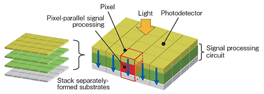
Figure 6-1. 3D integrated imaging device
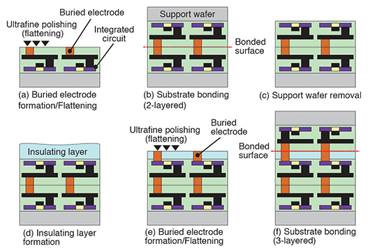
Figure 6-2. Multilayering process
■RGB-stack-type image sensors
We are conducting research on RGB-stack-type image sensors with the goal of realizing a single-chip color camera that is small, lightweight and highly mobile. These sensors consist of alternating layers of organic photoconductive films (organic films) sensitive to each of red (R), green (G) and blue (B) and thin-film-transistor (TFT) arrays for reading the signals generated from each organic film. In FY 2018, we worked to miniaturize TFT arrays to achieve a high-definition device.
The conventional TFT array used indium−gallium−zinc oxide (IGZO) for its semiconductor and had an etch-stop structure with a layer for protecting the semiconductor during the processing of the source and drain (S/D) electrodes (Figure 6-3 (a)). This structure, however, needed to be simplified to further miniaturize the TFT array. We therefore employed a back-channel-etch structure (Figure 6-3 (b)), which can eliminate the barrier layer and shorten the TFT channel length compared with that for the etch-stop structure. Since the S/D electrodes need to be processed directly on the semiconductor for this structure, we used indium−tin−zinc oxide (ITZO) semiconductor material, which has tolerance against electrode formation process. By introducing the above fabrication method and material, we developed a prototype TFT with a channel length of 2 μm, shortened from conventional 6 μm, and demonstrated that it achieved an ON-OFF ratio of 108 or more, which is sufficient for a signal readout TFT for image sensors. Using this TFT, we successfully miniaturized the pixel pitch of the signal readout TFT array from 50 μm to 20 μm (Figure 6-4)(2), showing the feasibility of a high-definition RGB-stack-type image sensor.
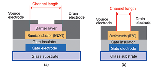
Figure 6-3. (a) Etch-stop structure TFT and (b) back-channel-etch structure TFT
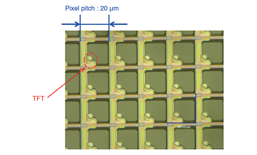
Figure 6-4. Microscope image of prototype TFT array
■Planer-type photoconductive film structure for solid-state image sensor with ultra-high sensitivity
In 2.2, we described our research on an 8K solid-state image sensor overlaid with a multiplier film for 8K cameras with high sensitivity. This device applies a voltage in the film thickness direction to form electric fields necessary for multiplying electric charges using avalanche multiplication phenomenon in the film (Figure 6-5 (a)) and thus aims to achieve an electric charge multiplication factor of about 10 times. While the electric field in the film needs to be further strengthened to increase the multiplication factor for future devices with ultra-high sensitivity, there is a limit to the voltage that can be applied to a film overlaid on a solid-state image sensor, making it necessary to reduce the thickness of the multiplier film in the case of the conventional structure. However, the thinner the film is, the less light can be absorbed, deteriorating the use efficiency of light. To solve this problem, we began researching a new device structure that can strengthen the inner electric field without depending on the film thickness (Figure 6-5 (b)). This structure can obtain an electric field which is laterally strong in the film by forming an electrode that applies a voltage (anode) in the same plane as a pixel electrode (cathode). This should make it possible to achieve a high electric charge multiplication factor without deteriorating light absorption characteristics while maintaining the thickness of a photoconductive film.
In FY 2018, we estimated the electric field intensity in the film necessary for achieving an electric charge multiplication factor of about 100 times on the basis of results of preliminary experiments and investigated an electrode structure for obtaining a desirable electric field intensity through simulations using electric field analysis. Figure 6-6 shows an effective electrode structure that we obtained from the analysis. Since the size of a single cathode-anode pair is expected to be very small, we used multiple cathode-anode pairs to constitute one pixel and arranged many sets of a cathode surrounded with an anode with a minute distance of submicron (0.1 μm or less) in between. We found that a strong electric field (108 V/m) for achieving a multiplication factor of about 100 times can be formed near the cathodes uniformly by optimizing the electrode size using this electrode structure.

Figure 6-5. Structure of image sensor overlaid with multiplier film
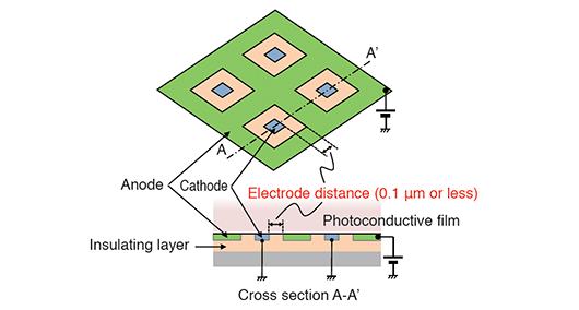
Figure 6-6. Electrode structure used for analysis
| [References] | |
| (1) | M. Goto, Y. Honda, T. Watabe, K. Hagiwara, M. Nanba, Y. Iguchi, T. Saraya, M. Kobayashi, E. Higurashi, H. Toshiyoshi, T. Hiramoto: "Design of Three-Layered Pixel-Parallel Image Sensors," The 79th JSAP Autumn Meeting, 19p-432-7 (2018) (in Japanese) |
| (2) | Y. Hori, T. Takagi, T. Sakai, M. Nakata, H. Sato, H. Ohtake and S. Aihara: "Miniaturization of TFT readout circuit for organic image sensor," ITE Annual Convention, 13C-1 (2018) (in Japanese) |