Research Area
2.2 Cameras
■1.25-inch full-featured 8K three-chip camera
With the aim of making a full-featured 8K SHV camera more compact and practical, we prototyped a full-featured 8K three-chip camera using a 1.25-inch optical format(1) (Figure 2-2). As image sensors, we used three 1.25-inch 33-megapixel CMOS image sensors supporting a 240-Hz frame frequency (that we developed in FY 2017) for RGB signals. We employed a system that performs sensor driving and signal processing all at 240 Hz and outputs full-featured 8K signals with a 120-Hz frame frequency by applying two-frame averaging at the last stage of signal processing in the camera control unit (CCU). This enabled the camera to be also used as an 8K 4× high-speed camera. To transmit image sensor signals driven at 240 Hz from the camera head to the CCU, we used the newly-developed optical transmission interface that can transmit signals of 448 Gbps in total over four optical fibers. Using a bidirectional wavelength division multiplexing technology, the interface can transmit 40-Gbps signals from the CCU to the camera head, which enables the transmission of return video signals with higher resolution to the viewfinder. The camera head and the CCU are connected by a cable including four optical fibers. The prototype camera head weighs 18 kg and the CCU weighs 37 kg, in the 8-RU size, both of which are less than half the size and weight of those of a conventional 8K three-chip camera.
We verified the effect of a noise reduction technology that we implemented on the 1.25-inch 33-megapixel image sensor(2). The image sensor that we developed contains a folding-integration analog-to-digital converter (ADC) with a three-stage pipelined ADC architecture, and multiple sampling operations in the folding-integration ADC reduced noise. There is a limit to the number of samplings that can be performed during driving at a 120-Hz frame frequency. We therefore built a simulation model to investigate the relationship between the number of samplings and noise and estimated the noise reduction effect of this method. The calculated results closely agreed with measured values and indicated that six sampling operations, which can be performed in 120-Hz driving, are sufficient for noise reduction. This research was conducted in cooperation with Shizuoka University.
To realize autofocus (AF) function for 8K cameras, we developed a method for estimating the distance to the object precisely and with a small amount of calculation by using on-chip phase detection(3). The on-chip phase detection system uses the amount of shift in images that is obtained from phase-difference detection pixels implemented on the image sensor. Applying complex analysis using rectanglar basis functions for phase calculation reduced the computation volume significantly compared with conventional distance estimation methods and achieved high-precision distance estimation.
■8K slow-motion system
To enable 8K slow-motion imaging in the production of sports and other programs, we developed an 8K slow-motion system that consists of an 8K high-speed camera and an 8K slow-motion recorder/player.
We added high-speed capture modes to our 1.25-inch full-featured 8K camera to achieve the 8K high-speed camera that supports a 4× capture mode (4:4:4 color sampling, capture at a 240-Hz frame frequency) and an 8× capture mode (4:2:0 color sampling, capture at a 480-Hz frame frequency). We also upgraded a slow-motion recorder/player supporting 8K 4× speed(4), which we prototyped in FY 2017, to make it able to support signal input of up to 8× speed (480 Hz) in agreement with the output of the high-speed camera (Figure 2-3). We also added a frame interpolation mode using two-frame averaging to the signal output function to enable smooth slow-motion video reproduction. We used this slow-motion system for the 8K live program production of international sport events and exhibited it at international exhibitions such as the NAB Show 2018 and IBC 2018.

Figure 2-2. 1.25-inch 8K three-chip camera head
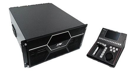
Figure 2-3. 8K slow-motion recorder/player and controller
■8K solid-state image sensor overlaid with multiplier film
The sensitivity of 8K SHV cameras decreases as they become more compact and support higher frame rates because the amount of light incident on each pixel of the imaging device decreases. As a drastic solution to this problem, we are developing a high-sensitivity solid-state image sensor overlaid with a photoconductive film (multiplier film) on a CMOS circuit for reading signal charges (Figure 2-4). The multiplier film can obtain the effect of electric charge multiplication by only applying a low voltage. In FY 2018, we worked to improve the image quality of the 8K solid-state image sensor overlaid with a multiplier film that we prototyped in FY 2017 and investigated ways to reduce the noise of an 8K CMOS circuit on which a multiplier film is overlaid.
Previously, crystalline selenium films that constitute multiplier films were formed by immediately heating amorphous selenium, in which atoms are arranged irregularly, at high temperature. However, the degradation of surface flatness and the internal stress of the film those result from sudden grain growth caused the image quality degradation of the sensor such as increased dark current and pixel defects. To address this problem, we introduced a two-step annealing method that heats selenium at low temperature to crystallize it briefly and then heats it again at high temperature for recrystallization after depositing an electron blocking layer and others on the crystallized selenium. This method successfully suppressed the degradation of image quality (Figure 2-5)(5)(6).
To increase the sensitivity of image sensors overlaid with multiplier films, it is important not only to multiply electric charges in the film but also to reduce the noise of the CMOS circuit. We therefore clarified the mechanism of dark current generation in the floating diffusion layer (i.e., a capacity for accumulating electric charges generated in the film) in the CMOS circuit and adopted a new structure that prevents the injection of dark current into the floating diffusion layer from the outside. We confirmed that this can reduce the shot noise of dark current to 1/8 that of the conventional structure(7). We also began prototyping test circuits with the aim of reducing noise that occurs when electric charges accumulated in the floating diffusion layer are reset after signal readings (reset noise) and improving the charge-voltage conversion gain.
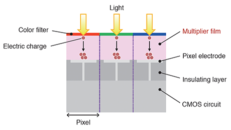
Figure 2-4. Structure of solid-state image sensor overlaid with multiplier film
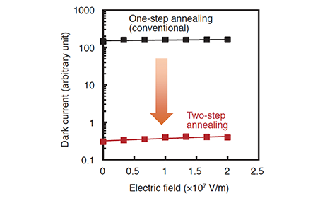
Figure 2-5. Dark current characteristics of device
| [References] | |
| (1) | R. Funatsu, T. Kajiyama, T. Yasue, K. Kikuchi, K. Tomioka, T. Nakamura, H. Okamoto, E. Miyashita and H. Shimamoto: "8K 240-Hz full-resolution high-speed camera and slow-motion replay server systems," IBC 2018 Conference (2018) |
| (2) | K. Tomioka, T. Yasue, R. Funatsu, T. Matsubara, T. Kosugi, S. W. Jun, T. Watanabe, M. Nagase, T. Kitajima, S. Aoyama and S. Kawahito: "Noise suppression effect of folding-integration applied to a column-parallel 3-stage pipeline ADC in a 2.1μm 33-megapixel CMOS image sensor," IS&T International Symposium on Electronic Imaging, IMSE-367 (2019) |
| (3) | H. Okamoto, R. Funatsu and H. Shimamoto: "A Proposal of Distance Estimation Method from Images," ITE Annual Convention 2018, 14C-4 (2018) (in Japanese) |
| (4) | T. Kajiyama, K. Kikuchi, R. Funatsu, E. Miyashita and H. Shimamoto: "8K240fps slow-motion replay server," ITE Annual Convention 2018, 31C-3 (2018) (in Japanese) |
| (5) | S. Imura, K. Mineo, K. Miyakawa, M. Nanba, H. Ohtake and M. Kubota: "Fabrication of polycrystalline selenium with high crystallinity and surface flatness using lateral grain growth by the effect of surface capping," Ext. Abstr. of the 65th JSAP Spring Meet., 17p-P3-1 (2018) (in Japanese) |
| (6) | S. Imura, K. Mineo, Y. Honda, T. Arai, T. Watabe, K. Miyakawa, M. Nanba, H. Ohtake and M. Kubota: "Reduction of pixel defects in stacked 8K image sensors using crystalline selenium films grown by two-step annealing," ITE Annual Convention 2018, 12C-4 (2018) (in Japanese) |
| (7) | T. Arai and H. Ohtake: "Evaluation of the dark current of three-transistor pixel circuits for 8K image sensors with a photoconductive layer," ITE Annual Convention 2018, 12C-5 (2018) (in Japanese) |