Content Production Technologies Bringing New Viewing Experiences (3 of 3)
High-speed Imaging Technology
Research Engineer, Advanced Television Systems Research Division
YASUE Toshio
NHK STRL is conducting research and development on future broadcast media technologies such as AR/VR, 3D television, and haptic presentation technologies. As part of these technologies, we have on-going research on production technologies to improve the expressiveness of video and sound produced by current televisions. In this series, we introduce content production technologies that will bring new viewing experiences, relentlessly pursuing higher realism in video and sound and achieving production not previously possible.
What is high-speed imaging technology?
High-speed imaging captures more frames per second so that fast-moving subjects can be portrayed smoothly, or so fast motions can be analyzed. BS4K and BS8K broadcast at 60 frames/s, so to produce smooth slow motion video in TV program (mainly for sports programs), the video must be captured at an even higher frame rate.
There are technologies that use specialized cameras and other equipment to perform high-speed imaging at up to 10,000 frames/s or more, but they are constrained to lower resolution and several seconds of recording time. On the other hand, the technology we are developing is able to capture several hundred frames per second over long recording times. We have developed an 8K 4x slow-motion system that can record continuously at 240 frames/s, and has been used for many programs (Fig. 1). Here, we will introduce an image sensor technology, which is a key component of the camera.
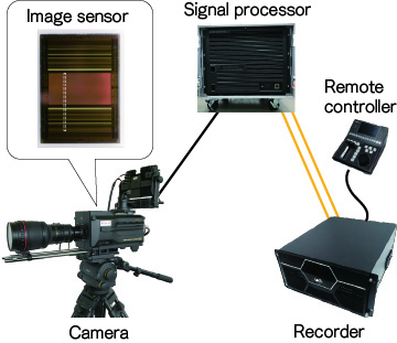
Image sensor technology
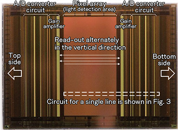
The image sensor is a semiconductor chip that converts the light collected by a lens for each pixel into an electrical signal (Fig. 2). It plays an important role determining the quality of the image since it is the entry point of the signal. Due to characteristics of semiconductor circuits, it is difficult to achieve high-speed operation, low noise and low power consumption, all at the same time. Based on earlier research results, we developed the technology below, improving the balance among these three performance factors.
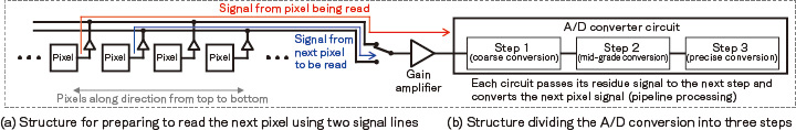
One technique*1 that is effective in suppressing noise is to sample the signal multiple times and average the results, but repeated sampling takes time, making it harder to achieve high speed. To achieve both low noise and high speed, we implemented two signal lines for each pixel column to transfer signal from the pixel to the gain amplifier, and used both alternately for conversion, improving utilization of time (Fig. 3 (a)).
A/D conversion*2 accounts for a large share of power consumption, so we developed A/D conversion circuits that divide the conversion into three steps: with coarse, medium and precise accuracy, optimizing the circuits for each step and processing in parallel (Fig. 3 (b)). The circuit is capable of operating at high speed, performing over a million conversions per second to handle high-speed imaging, while maintaining power consumption low enough for continuous operation.
Future prospects
A feature of immersive media that we are researching is the use of a wider field of view to increase the sense of immersiveness. This could require resolution that exceeds that of even 8K, and technologies developed for high-speed imaging will be useful as more pixels are used. We will continue R&D in pursuit of image quality for immersive media.