Development of Flexible Liquid Crystal Displays
Hiroto SATO and Hideo FUJIKAKE
We have been developing fast-response ferroelectric liquid crystal (FLC) devices using fine polymer walls and fibers for future flexible TV displays with excellent portability. In the device fabrication process, the molecularly aligned polymer walls and fibers, which stabilize thin plastic substrates and FLC alignment respectively, are sequentially formed by polymer segregation using two-step ultraviolet irradiation of a molecularly aligned FLC/monomer solution. A fabricated device exhibited a grayscale electro-optic characteristic with a high contrast ratio of over 100:1 and a fast response of less than 1 ms. A4-size flexible FLC displays were fabricated with a new plastic-substrate based process that uses printing and transfer techniques. Full-color moving images were displayed on the FLC matrix panel, which was driven by an active technique using an external switch transistor array based on the field-sequential-color method.
1. Introduction
The advent of digital broadcasting and portable receivers makes it feasible to receive and view television broadcasts without restriction to location or time, and consequently, display devices based on new concepts will be in demand. These devices will go beyond the conventional fixed-location system, and people will utilize them in a wide range of environments. Among the potential advanced display devices, we anticipate that a lightweight flexible display that could be rolled up would have a wide range of applications, including roll-up portable displays and displays with large, paper-thin screens. While a number of flexible devices, including those based on liquid crystal and organic EL, have been proposed, liquid crystal (LC) devices lend themselves to various transmissive, reflective, and trans-reflective display schemes. Hence, the LC devices have good potential for use in a flexible display device that would provide excellent visibility in a wide range of indoor and outdoor lighting environments. However, the fabrication of a flexible display system for a high-picture-quality portable television will require the development of a technique to place fluid-body liquid crystal between flexible plastic substrates at a uniform thickness, as well as the use of a liquid crystal material with fast enough response for high-quality moving image presentation.
With the aim of constructing such a flexible display system for moving image presentation, our laboratories have been studying a flexible liquid crystal display using a composite film of fast-response ferroelectric liquid crystal (FLC) and polymer (synthetic resin). This report describes the status of our work on this flexible liquid crystal, especially focusing on the composite film fabrication techniques.
2. Structure and Operation Principle of Film Display Device Using Liquid Crystal
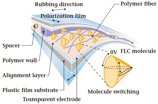
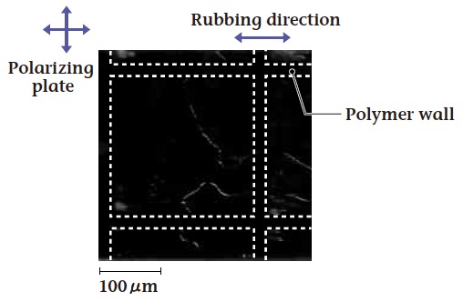
Figure 1 illustrates the basic structure of the film display device using LC. The device is composed of a composite film of FLC and polymer fiber placed between two plastic substrates with transparent electrodes. The composite film is formed with lattice patterned polymer walls, which adhere to the substrates and maintain a uniform thickness for the composite film, sustaining the fragile liquid crystal molecular alignment even when the device is bent. The molecular alignments of two types of polymer are controlled in the rubbing direction by the polyimide alignment layer, which is deposited and rubbing processed over the transparent electrode. Although FLC molecules tend to tilt from the rubbing direction of the alignment layer, we succeeded in aligning the FLC molecules in the rubbing direction by anchoring of the fine polymer fibers. One of the transmission axes is set in the FLC molecular alignment direction, which is the rubbing direction.
Without a voltage at the transparent electrodes, incident light, which is linearly polarized at the polarizing film, is absorbed at the polarizing film on the output side, since no effect is received from the refraction index anisotropy of the FLC molecules. On the other hand, when a voltage is applied between the transparent electrodes, the FLC molecules rotate on the conical surface and are tilted from the optical transmitting axes of the polarizers, resulting in the light being transmitted through the output side polarizing plate. As birefringence effect of the FLC molecules depends on the title angle, whose direction and angle can be controlled by adjusting the voltage, it becomes feasible to perform analog modulation of the transmitted light.
Linearly polarized incident light at the polymer walls with the molecular alignment in the rubbing direction is not affected by birefringence polymer; thus those wall portions stay black.
3. Composite Film Fabrication Method
3.1 Two-step UV irradiation method
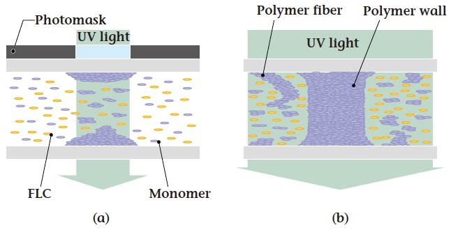
A conventional LC display is not constructed on the premise of it being bent during use. It thus requires no special internal walls. Therefore, the device structure shown in Figure 1 necessitated the development of a new technique to form two small polymer structures designed for separate functions inside the FLC. The authors and their research group have devised the following fabrication method, in which UV-curable monomer material is irradiated with UV light in two phases.
The first step involves placement of the FLC/monomer solution between two plastic substrates, to which localized patterned exposure is performed using UV light over a photomask, while heating the solution to attain a state where the LC molecules and monomer molecules align in the rubbing directions (nematic phase). The polymer walls are formed in the exposed area through polymerization of a large number of monomers upon UV light irradiation (Figure 2 (a)). This is because even unreacted monomers in the un-exposed areas are affected by the thermal effect. They diffuse to the exposure area to be sequentially reacted by the UV light, thereby accelerating polymer deposition and growth.
This step is followed by uniform UV irradiation without the photomask while the device is temperature controlled to maintain the nematic phase of the solution, except for the wall area (Figure 2 (b)). This exposes all the unreacted monomers in the un-exposed area that are left over from the polymer wall formation, causing the distributed formation of small polymer fibers in the LC.
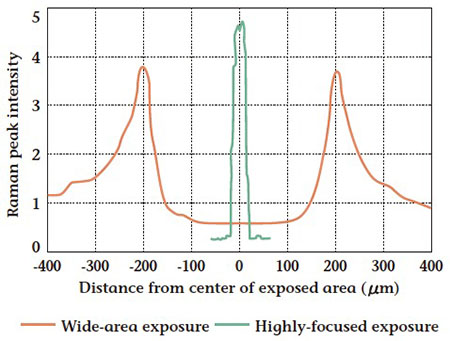
Before the two polymer structures could be fabricated using the two-step UV irradiatio method, we had to determine the deposition conditions for highly dense walls under localized exposure. For this reason, we evaluated the deposited polymer concentration in-plane distribution using the two-step exposure method. This spectroscopic measurement (micro Raman spectroscopy) enabled us to determine the respective LC and polymer concentrations. The Raman scattering peak intensity of polymer against LC in the localized exposure areas is illustrated in Figure 3. The Raman intensity reflects the polymer concentration. Wide-area exposure causes highly dense polymer formation only at the border with the unexposed area, and does not result in uniform formation. It was clarified that highly focused exposure (exposure diameter: 40 µm) can adequately supply monomer materials flowing from unexposed sections through molecule diffusion to even the central region, and high-density polymer can be deposited over the entire exposure area. Based on these experimental results, the following experiment was conducted with a grid pattern line width of 30 µm or less.
3.2 Polymer molecule alignment control
The formation of polymer with molecular alignment in the rubbing direction requires that the FLC/monomer solution be maintained in the nematic phase. The fact that the temperature range for the nematic phase narrows as the monomer concentration decreases at the wall formation requires that the solution temperature be adjusted according the monomer concentration. This means that monomer consumption in the solution at the time of wall formation causes the LC to tilt, which in turn causes the monomer to tilt with the LC. The molecular alignment of the deposited polymer becomes inclined. Figure 4 shows a polarizing microscopic observation of the solution (monomer: 30%) in the nematic phase, following patterned exposure (40 mW/cm2) at a constant 40 ℃. It shows an inclined LC alignment from the rubbing direction in the vicinity of walls that is due to deposited polymer with a tilted molecular alignment. To stop this from happening, we performed patterned exposure while raising the temperature to maintain the homegeneous alignment of the solution. This prevented polymers with inclined alignment from being deposited, and made the liquid crystal alignment uniform in the rubbing direction.
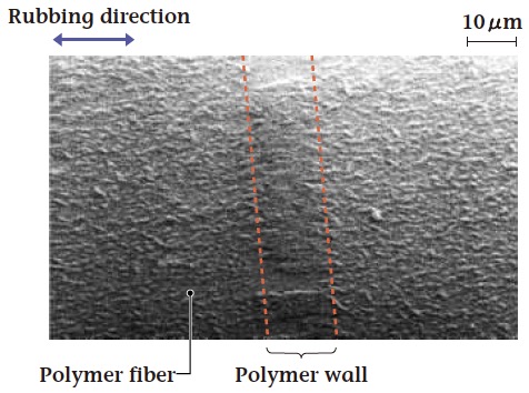
Figure 5 shows a scanning electron micrograph of the formed polymer structures. It indicates a molecular alignment of the polymer walls and fibers in the rubbing direction. The molecularly aligned polymer fibers can control the alignment of the FLC molecules in the rubbing direction. Polarization microscopic observation of a composite film verified the liquid crystal's uniform molecular alignment even near the walls, as well as a significant reduction in light leakage (approximately 1/5) (Figure 6).
The above method requires precise and complicated temperature management to maintain the nematic phase during wall formation. We are devising a technique to broaden the nematic phase temperature range by adding a small amount of nematic LC material to the FLC. It was determined that this technique gives a good black level with uniform LC molecular alignment near walls, even with a flat-temperature localized exposure. This technique is extremely useful for fabricating a large-area devices, which normally have temperature uniformity problems.
Based on these evaluations and with a view toward ensuring a secure aperture ratio and mechanical strength, we determined the width of the polymer walls to be 20 µm at 250 µm intervals.

4. Electro-Optic Characteristics
Figure 7 is a measurement example for a prototype device fabricated with the above method. A light modulation property is obtained wherein the transmittance is symmetrical to the voltage polarity change, making analog modulation through variable control of the applied voltages. The contrast ratio is 100:1 or higher. An investigation of the effect of the polymer on LC molecular behavior through the use of Raman spectroscopy and a reduction in the size of the formed polymer led to low voltage operation (several V) suitable for TFT driving. Pulse voltage impression showed a response characteristic of 1 ms or less over every grayscale level, including the rise and decay times, which is fast enough for moving image presentation.
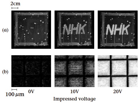
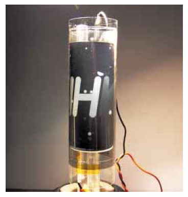
Figure 8 (a) shows the result of light modulation with a voltage over a device (10 cm square). It indicates uniform grayscale operation. Such a grayscale display function comes from sequential changes in LC alignment based on voltage intensity, as captured in the polarization microscopic images at Figure 8 (b). We also conducted bending tolerance tests. The FLC alignment supported by the polymer walls for bonding and maintaining the substrates can withstand the device being bent to a radius of 1 cm or less. Uniform display was possible even at a bend radius of 2 cm or smaller when the device was placed between polarizing plates at the time of voltage impression (Figure 9).

5. Fabrication of Larger Display Devices
To construct a large screen display that can be rolled up, the thickness uniformity of the LC layer must be maintained relative to the flexible plastic substrates. This requirement makes it difficult to apply a conventional LC display fabrication method based on LC injection. For this reason, we developed the large-area fabrication process described below, which incorporates a printing method, which is advantageous for a large area, and laminating technology using the substrate flexibility. Figure 10 outlines the fabrication method for large flexible devices.
This method employs glass substrate transfer technology to form transparent electrodes and a black matrix over plastic substrates (Figure 10 (a)-(b)). The transfer method's use of a glass substrate during formation and the patterning of the transparent electrodes and black matrix (photolithographic method), as in conventional LC display fabrication, requires no consideration of the dimensional stability of the plastic substrates.
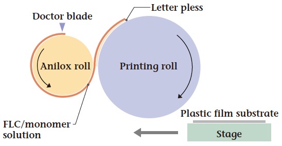
An FLC/monomer solution is then applied to the plastic substrate along with spacer particles (1.5 m diameter) that determine the thickness (Figure 10 (c)). Any lack of uniformity in the thickness of the mixture layer applied during this process generates display irregularities in the fabricated device. The use of a flexographic technique, which can attain a uniform layer even on a large flexible substrate, led to the FLC/monomer solution film application over plastic substrates (Figure 11). During the process, we optimized the pressure of the letter press that contacts the substrate, which is fixed on the stage, by adjusting the height of the printing roll. The resulting A4-size film had an even thickness.
The final steps involved laminating the film with another plastic film substrate by using a pressure roller (Figure 10 (d)), followed by forming polymer walls and fibers within the LC by using a two-step UV irradiation method (Figure 10 (e)-(f)). The prototype device had uniform molecular alignment, and the molecular alignment could be maintained when the device was bent with a 2 cm radius even after it was placed between polarization films.

6. Examination of Matrix Display
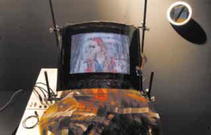
To verify the moving image display ability of the panel, we fabricated a prototype A4-size flexible color display equipped with a flexible backlight sheet, which contained a large number of LED chips over the surface of a polyimide film circuit substrate. We attempted to obtain matrix driving based on a field sequential color technique, with which the color display function can be obtained through a small number of pixels, by using the fast response characteristics of FLC. The field sequential color display scheme realizes a full-color display through synchronization of individual pixels on the LC panel with the three primary color intermittent lighting from the LED array, along with high-speed analog modulation (180 Hz) of the primary color lights. Instead of a large area of thin transistors on a plastic substrate, which is currently difficult to do, this experiment used individual pixels on the LC panel, driven separately using a matrix circuit with transistors installed in an external driver (external transistor array).
Figure 12 shows a display example of this prototype flexible FLC display (96 × 64 pixels). The picture is of a stable full-color moving image, with the device in a curved state.
7. Conclusion
We used a polymer formation method in which UV light is irradiated on a mixture of molecular alignment controlled LC and monomer in two phases to fabricate an FLC polymer composite film with high curvature tolerance and fast response capability. A newly developed large area fabrication technique based on a transfer technique and a flexographic printing technique was used to fabricate an A4-size flexible FLC display device. Installation of a flexible three primary color backlight on a flexible display panel for external transistor array driving led to a successful full-color moving image presentation. Our ongoing research includes a driving experiment based on organic TFT fabricated over plastic substrate. Through these efforts, we hope to improve LC characteristics and create higher definition pixels.
We would like to express our appreciation to Mr. Tadahiro Furukawa of Kyodo Printing Co., Ltd. for his help with the plastic substrate processing.