300,000-pixel Ultrahigh-speed High-sensitivity CCD and a Single-chip Color Camera Mounting This CCD
Hiroshi OHTAKE, Tetsuya HAYASHIDA, Kazuya KITAMURA, Toshiki ARAI, Jun YONAI, Kenkichi TANIOKA, Hirotaka MARUYAMA, and Takaharu ETOH
We have been developing ultrahigh-speed, high-sensitivity broadcast cameras that are capable of capturing clear, smooth slow-motion video even in limited lighting, such as at professional baseball games played at night. Earlier, we developed a broadcast color camera using three 80,000-pixel ultrahigh-speed, high-sensitivity CCDs. This camera had about ten times the sensitivity of standard high-speed cameras, and enabled an entirely new style of presentation for sports broadcasts and science programs.
We are continuing with this work with the aim of improving the camera's resolution. In this paper, we discuss our experimental development of a new ultrahigh-speed high-sensitivity CCD that increases the number of pixels four-fold to 300,000 pixels, as well as the development of a single-chip color camera that mounts this CCD.
1. Introduction
The recent advances in cameras' ability to capture fast-moving phenomena that cannot be perceived clearly with the naked eye and to represent these in slow-motion video are drawing interest not only for scientific measuring purposes but also for broadcasting applications.
Many of the conventional high-speed camera systems incorporate a CMOS imaging device, which can read out signal charge at high speed by using an X-Y matrix switching scheme. However, there are problems with CMOS imaging devices; they require especially intense lighting to obtain video with a good SN ratio during high-speed shooting with a short exposure time because they are affected by noise and have inadequate sensitivity. This requirement has made it difficult to perform high-quality high-speed shoots for relay broadcasts of nighttime sports events at facilities with inadequate on-site lighting.
We have constructed a three-CCD ultrahigh-speed high-sensitivity color camera based on a special 80,000-pixel CCD with high operational speed and excellent sensitivity, and have used this camera in experimental relay broadcasts of professional baseball games and golf tournaments. The experimental broadcasts proved the camera to be a powerful tool for shooting new forms of video expression; for instance, it captured extremely vivid footage of a ball's impact with the bat during a baseball game.
With a view toward developing an ultrahigh-speed broadcasting camera with superior resolution and functionality to the previous one, we recently fabricated a 300,000-pixel ultrahigh-speed high-sensitivity CCD. This is approximately a four-fold increase in pixels from the previous model. The new CCD has a unique structure with internal memories, making it as difficult to manufacture as a 40,000,000 pixel CCD when these memories are regarded as a type of pixel. To ensure an adequate fabrication yield, a prototype CCD with half the number of pixels (150,000) was initially designed and constructed, and through development of a technique that enables cutting along the edge of the CCD and bonding two CCDs together with a high degree of accuracy, we created a 300,000-pixel CCD. This new ultrahigh-speed CCD was equipped with an on-chip color filter in the single-chip color camera.
In the following, we will describe the principle behind our new CCD. After that, we will describe how the prototype 150,000-pixel CCD was engineered with a view toward constructing a 300,000-pixel CCD. We will also discuss the element technologies of the CCD and the experimental single-chip camera equipped. The results of an imaging experiment using this camera are also reported.
2. Ultrahigh-speed High-sensitivity CCD Principle
The ordinary CCD shown in Figure 1 (a) must carry its signal charge, which is generated by incident light in a photodiode, to an outside CCD via a long transmission channel at 1000 stages per frame (for every single shot image). This arrangement significantly restricts shooting speed. In contrast, our ultrahigh-speed CCD directly connects the memory for signal recording to the photodiodes for individual pixels, as illustrated in Figure 1 (b). Therefore, only a single stage is involved in the signal charge transfer per frame, and this enables a maximum shooting speed of 1,000,000 frames per second. The larger photodiode area together with a low noise CCD design helps to increase sensitivity to approximately ten times that of a conventional CMOS image sensor. It has a drain section* at the last CCD memory stage where old signals, which had been transferred over 144 stages, or equal to the number of CCD memories, can be discharged sequentially via a circuit to outside the CCD. This sequential rewriting operation assures the capture of the decisive moment when a high-speed phenomenon occurs.

3. 150,000-pixel Ultrahigh-speed High-sensitivity CCD
We engineered and test manufactured a 150,000-pixel ultrahigh-speed high-sensitivity CCD with the aim of constructing a broadcasting camera system with higher picture quality, functionality, and speed. Table 1 compares the specifications of the previous 80,000-pixel ultrahigh-speed CCD and the new 150,000-pixel one.
| Previous ultrahigh-speed CCD | Newly-designed ultrahigh-speed CCD | |
|---|---|---|
| Pixel number | 312×260 (Approx. 80,000 pixels) |
360×413 (Approx. 150,000 pixels) |
| Maximum shooting speed | 1,000,000 fps | 1,000,000 fps |
| Shooting recording frames | 103 frames | 144 frames |
| Continuous shooting mode (external memory use) |
Unavailable | to 1,000 fps |
| Pixel size | 66.3 µm × 66.3 µm | 50.4 µm × 50.4 µm |
| CCD memory area | 5.1 µm × 5.1 µm | 3.0 µm ×3.6 µm |
| Charge handling capacity | 25,000 electrons | 11,500 electrons |
3.1 More pixels
With regard to increasing pixels, we reexamined the layout of individual CCD parts in light of the latest processing data provided by CCD manufacturers. The first step was to reduce the CCD transfer channel width from the previous 5 µm to 3 µm. To prevent this adjustment from causing any performance degradation, such as in transfer efficiency, we had to consider the design very carefully and used a device simulator to ensure smooth electrical potential gradient connections between parts.
Next, we tried to reduce the amount of metal wiring in the upper part of a pixel. High-speed signal charge transfer, which needs to be done in the photodiode section and CCD memories in an ultrahigh-speed CCD, requires low wiring resistance for the driving voltage supplying the CCD electrodes. We used a metal wire material that had low resistance to the driving voltage supplying the CCD electrodes (note that conventional wiring is made of the same material as the CCD electrode, polysilicon), and by installing the wire in the upper part of the pixel to attain the shortest distance from the CCD electrode for connection. However, the distance between the metal wires themselves decreases as the pixel area decreases, and this can lead to inter-electrode shorting. The lower fabrication yield that would result from such a problem prompted us to investigate the possibility of reducing the amount of metal wiring. The results of our simulation revealed that exclusive metal wiring, which had been required at the drain electrode for performing a continuous rewriting, could be eliminated by optimizing the impurity concentration distribution within the CCD and by using driving voltage control. This made it feasible to reduce the pixel area without shortening the distance between the metal wires, and enabled us to integrate 150,000 pixels within the target area.
3.2 Recording frame number
We reduced the size of the CCD memory to the minimum design rule value of 3.0 µm × 3.6 µm to increase the number of frames recorded during shooting (CCD memory number) from the 103 frames of the 80,000-pixel CCD to 144. In consideration of a possible saturated charge decline induced by the smaller CCD memory area, the amount of saturated charge was simulated and analyzed. The assumption of ten noise electrons for this CCD to secure a 10-bit dynamic range gives a saturated charge of 10,000 electrons or higher, so we made that our target. The simulations indicated a saturated charge of approximately 11,500 electrons, which exceeds the 10,000 electron target.
3.3 Extended-time continuous imaging
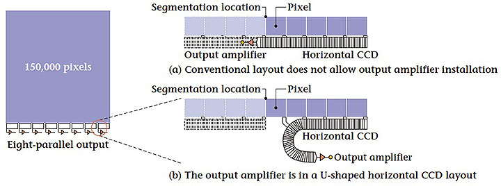
The CCD was designed to be capable of extended-duration continuous imaging using an external memory. The structure of the horizontal CCD is divided into eight segments to perform high-speed parallel signal readout. The conventional layout shown in Figure 2 (a) does not have enough space to install output amplifiers in the respective segments. This issue was resolved by arranging the stages close to the end of the horizontal CCD in a U-shape, as shown in Figure 2 (b).
3.4 Buttable Structure
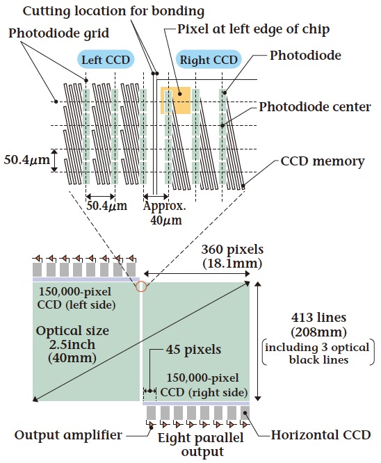
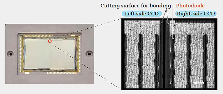
The CCD has a special structure in which every pixel has a large area photodiode directly connected to the CCD memory. This structure significantly reduces the fabrication yield, as more pixels indicate an increase in area. To solve this problem, we incorporated a buttable structure in which multiple image sensors are bonded together to form a larger sensor. Figure 3 illustrates this buttable CCD structure. We arranged photodiodes at the left edge of the pixels of the 150,000-pixel CCD in such a way to ensure a cutting margin of 10 µm or greater between the photodiodes and the cut line for bonding.
4. Element Technologies for CCD Bonding
4.1 Accurate cutting technology
The photodiodes of the right and left bonded CCDs have to be centered at a pixel pitch of 50.4 µm. The cutting technology has to cut the edge of a CCD with a high degree of accuracy to face the other CCD. The cutting technologies for the silicon wafer include mechanical cutters with high-speed rotary blades and chemical cutting such as etching. We chose to use mechanical dicing using a high-speed rotary blade that is commonly employed in semiconductor processing. Figure 4 gives an overview of this dicing apparatus. A cut is made by rotating a thin film-shaped diamond grinding stone (i.e., diamond blade) at a high speed, toward which a wafer is moved on a highly accurate X-Y stage. This cutting process is employed in applications with an approximately 100 µm cutting margin between the device and the cutting location, and under the assumption that wafer chipping of 5 to 10 µm during cutting is too insignificant to affect device characteristics. However, the cutting margin of the 150,000-pixel CCD was only a little over 10 µm, and this meant the cutting process might adversely affect the device characteristics. We conducted an experiment to determine the cutting conditions that would minimize chipping at the cut surface. We made a device cut close to a photodiode, and examined the extent of the damage (leak current) caused by the cutting process. Ordinary blade dicing leaves the upper portion of the cut surface at an obtuse angle (Figure 5 (a)), exposing the back surfaces of both CCDs and making accurate positioning difficult. This problem was solved by tilting the rotating shaft of the dicing apparatus approximately 1° (Figure 5 (b)).


4.2 Chipping and optimum cutting conditions
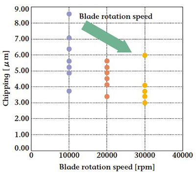
The best cutting conditions to minimize chipping included 1) grinding diamond diameter (blade model number: a smaller model number indicates a smaller grinding diamond diameter), 2) blade rotation speed, and 3) stage feeding speed. The amount of chipping was defined as the width of the largest chip taken from a post-cut cut surface, as observed with an optical microscope.
Figure 6 shows the relationship between grinding diamond diameter and amount of chipping. The blade rotation speed is 3000 rpm with a stage feeding speed of 0.5 mm/s. The figure indicates that a smaller grinding diamond diameter is more likely to yield smaller chips. Figure 7 illustrates the relationship between blade rotation speed and amount of chipping. The blade used in the experiment was model number 2030, and the stage feeding speed was 0.5 mm/s. The figure shows that a higher blade rotation speed reduces the amount of chipping. Figure 8 shows the stage feeding speed in relation to the amount of chipping. The model 2030 blade rotated at 3000 rpm. Less chipping was observed as the stage feeding speed decreased. These experiments revealed that the minimum amount of chipping is attained with a small grinding diamond diameter, maximum blade rotation speed, and slow stage feed.
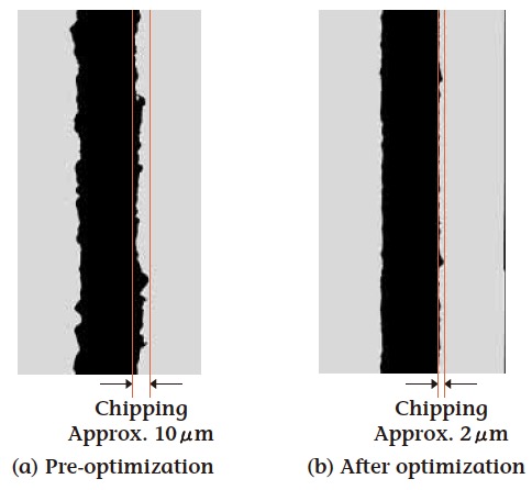
The microphotographic images in Figure 9 compare the cut surfaces under pre-optimized and optimized conditions. We succeeded in reducing the amount of chipping to approximately 2 µm.


4.3 Impact of proximate cutting on photodiode characteristics
The cutting technique causes some mechanical damage to the cut surface of a device, and we speculated that this damage still might have an impact on device characteristics, including the leak current. To evaluate the relationship between the cut location and diode leak current, we constructed the prototype diode shown in Figure 10. The leak current was measured at various cutting positions and using the n-type diffused layer standard (position 0). The results in Figure 11 indicate that no increase in leak current occurs when the distance between the n-type diffused layer and the cutting location is +4 µm or greater. This finding revealed that a CCD in which the distance from the cutting location to a photodiode was 10 µm or greater, which is sufficiently greater than the 4 µm threshold, would not suffer any influence from the dicing process.


4.4 High-accuracy positioning technique and prototype package fabrication
To position the two 150,000-pixel CCDs for bonding, we fabricated a high-accuracy positioning system based on a highly accurate stage using a piezoelectric device and a high-accuracy laser microscope. Figure 12 shows the configuration and a picture of this system. This system's positioning accuracy is 1 µm or less along the X-Y axis.
We also fabricated the packaging for a 300,000-pixel CCD. The ceramic package used in ordinary CCDs is manufactured in a calcination process, which is not suitable for an application that requires profile accuracy. Our CCD is designed for a future application with a micro lens, with a minimum in-plane vertical length of 5 µm or less to obtain uniform sensitivity. Thus, in addition to the regular package, we polished the base to an in-plane vertical length of 5 µm or less. We selected aluminum nitride substrate to be the base material that directly connects to the CCD. This material has good heat radiation characteristics and a linear coefficient of expansion similar to that of silicon. The package was designed to enable cooling with a Peltier device, and it had a rotationally symmetrical structure to accommodate the buttable CCD chip.
We used the high-accuracy positioning system to test manufacture a 300,000-pixel CCD. Figure 13 shows a post-packaging image of the chip and an enlarged image of its bonding area. The positioning system succeeded in pasting together right and left CCD photodiodes to an accuracy of 1 µm or less.

5. 300,000-pixel Ultrahigh-speed High-sensitivity Single-chip Color Camera
5.1 Camera configuration and operation
We incorporated an on-chip color filter (Bayer, RGB filter) with the 300,000-pixel ultrahigh-speed CCD to construct a prototype single-chip color camera system. The camera's external appearance is shown in Figure 14, and its specifications are listed in Table 2. The CCD has a diagonal length of approximately 40 mm, and this led to the installation of an F-mount lens. The F mount makes it feasible to use a wide range of low-cost commercial lenses, which means that the system to be easily used in a variety of subject conditions.
Figure 15 outlines the camera's configuration. Its mechanical shutter closes during the signal charge readout period following ultrahigh-speed shooting to prevent light from entering the charge transfer channel. The CCD driver consists of a driving field programmable gate array (FPGA) and a CCD driver, and it drives the CCD, the mechanical shutter control, and the trigger control. The signal processor is composed of an A/D, semiconductor memory, signal processing FPGA, and an HD-SDI generating circuit. The 16ch parallel read-out CCD output signals are processed in a 16ch parallel circuit configuration for the A/D to semiconductor memory for video signal storage. The signal processing FPGA handles the control of the A/D and memory, as well as 16ch signal synthesis processing and color processing.

| Image sensor | Ultrahigh-speed CCD |
|---|---|
| Pixel number | 720 pixel × 410 pixel |
| Aspect ratio | 15.9:9 |
| Device size | 40mm diagonally |
| Frame rate | 30 to 1,000,000 fps, 30 to 1,000 fps (using external memory) |
| Ultrahigh-speed shooting mode shooting frames |
144 frames |
| Recording time with external memory | Approx. 5 s at maximum (1000 fps) |
| Recording media outside the CCD | Semiconductor memory (Approx. 2 GB) |
| Video output | HD-SDI : 1 |
| External trigger input | TTL or switch closure |
| Lens mount | F mount |
| Dimension | 180 mm (W) × 150 mm (H) × 300 mm (D) |
| Camera weight | 5.2 Kg |
| Power consumption | Approx. 75 VA |

5.2 Camera operation
The camera has two shooting modes, an ultrahigh-speed mode that stores signals in inter-CCD memories, and a long-duration continuous high-speed shooting mode that performs parallel-readout of the CCD signals and stores them in an external memory device. These operational modes are respectively discussed in the following sections.
5.2.1 Ultrahigh-speed shooting mode
The ultrahigh-speed mode shoots at 30 to 1,000,000 frames per second. It stores the signal charge in the CCD's memory, allowing a recording time of 144 frames regardless of shooting speed setup.
In this mode, the camera goes into standby status when a driving pulse is generated at the CCD driving FPGA, based on a pre-set shooting speed. The 144 frame memories for recording initiate a repeated rewrite recording operation awaiting a trigger signal input. On receiving the trigger signal, rewrite recording stops and 144 frames worth of sequential ultrahigh-speed images are recorded in the CCD memory. This trigger signal can occur at an arbitrary position in the 144 frame sequence, allowing the recording to begin immediately before the target ultrahigh-speed phenomenon occurs. Following the shoot, the mechanical shutter is closed, and the stored signal charge inside the CCD is read out externally. The respective output signals are stored in semiconductor memory after A/D conversion processing. When the data transfer for an entire frame is complete, the data from the semiconductor memory is synthesized at the signal processing FPGA into an HD-SDI signal output. The processing time required from trigger to HD-SDI signal output is one second or less.
5.2.2 Long-duration continuous high-speed shooting mode
This mode the camera reads out high-speed parallel CCD signals and stores them in an external semiconductor memory. This enables continuous shooting at 1,000 frames per second or less over a duration depending on the semiconductor memory capacity.
The long-duration mode begins immediately after a CCD driving pulse for continuous shooting is generated at the CCD driving FPGA at a shooting speed determined in advance. The signal charge is sequentially read out using 16ch-parallel readout to a device outside the CCD. Individual output signals are stored in semiconductor memory after A/D conversion. The external memory is a semiconductor device with a 2 GB capacity, which is enough for storing approximately 5 seconds worth of images at 1,000 frames per second. After shooting finishes, data stored in this semiconductor memory is synthesized at the signal processing FPGA for post-color-processing HD-SDI signal output.
5.3 Imaging experiment
We evaluated the characteristics of the camera in imaging experiments conducted at baseball night games and indoor athletic performances.
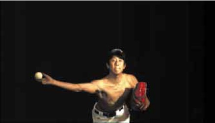
Figure 16 shows an imaging example of a baseball pitcher shot at 1,000 fps. In addition to this image, the camera successfully captured clear images of various decisive moments, including the ball leaving the pitcher's hand, the ball's rotation, the pitcher's pitching form, and the movements of the pitcher's arm and shoulder muscles. The enhanced resolution resulting from the 300,000 pixels contributed to a better depiction of the texture of his muscles than could be obtained with the previous 80,000-pixel ultrahigh-speed camera.
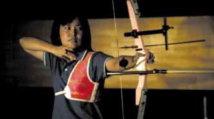
Figure 17 shows an example of shooting at 8,000 fps to capture the moment that an arrow is launched from an archery bow indoors. Indoor high-speed shooting had proved difficult with a conventional CMOS image sensor because of its low sensitivity. In contrast, the new camera's high sensitivity enabled it to clearly capture the moment when the bowstring pushed out the arrow.
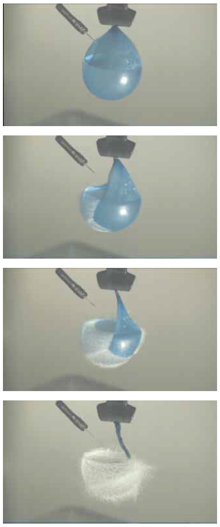
Figure 18 shows imaging at 16,000 frames per second to capture the moment when a water balloon bursts. The footage clearly shows how the rubber of the balloon tears and the water is released. It also shows how the water drops remain in the air even after the balloon has completely burst.
6. Conclusion
The 300,000-pixel ultrahigh-speed CCD was developed with the aim of constructing a camera that has a high enough picture quality and enough functionality for broadcasting applications. A 150,000-pixel CCD was initially engineered and fabricated to ensure an adequate fabrication yield, and techniques to dice and position two 150,000-pixel CCDs with a high level of accuracy were developed to bond the two chips into one with 300,000 pixels, which is four times the number of pixels of the previous model. A 16 segment structure for the CCD output was designed to enable long-duration continuous high-speed shooting using an external memory.
A single-chip ultrahigh-speed color camera was constructed by applying an on-chip color filter to the 300,000-pixel CCD. Imaging experiments using this prototype camera were performed at nighttime baseball games and indoor archery meets. The results indicated the camera had outstanding performance; it captured clear slow motion images with heightened detail and texture, including the dynamic muscular movements of a pitcher while pitching a ball; such images could not be feasibly captured with conventional high-speed camera systems under similar circumstances.
Our future work will involve installing a micro-lens array on a CCD to further enhance sensitivity with a view toward constructing a multi-chip ultrahigh-speed high-sensitivity color camera with an HDTV level of resolution and faithful color reproduction.